The optimal high frequency response for a 16x34 radiometer
video amplifier would be one that could render a 16x34 checker type image. If 4
frames a second are to be rendered, the signal of a pixel must be a square wave
of 4 x (34+blank)/2 Hz. The blank time is about 20% of the total, rendering a
frequency for the square wave of 85Hz. In order to get near to that ideal, we
need at least the 1st harmonic and even a bit of the 3rd.
Hence, the video amplifier must not roll off at less than150 Hz and should show
a sharp cut in order to reduce the RMS upper band noise.
The low end of the spectrum, in a simple approach, it should go all the way to DC. Any attempt to high pass the signal would introduce artifacts. If the DC were to be filtered away, in a column with bright spots, dark spots will be darker than in a column with no bright spots. Still, only changes from noise within a vertical scan degrade the image. Considering 4 vertical scans per second (2 ups and downs), the lower band limit will be 2 Hz while upper band, as mentioned above, must be above 150 Hz.
The current amplifier has a low pass RC of 10 ms (100 KW x 0.1 mF), or in the frequency domain 15.9 Hz 3 dB roll off frequency. That would bring down the relevant band for noise, but it is my opinion that this filter will blur the image and it should be modified to roll at 100 Hz. For the higher resolution (32x66) and 15 frames per second the band will shift to 1.9 to 1091 Hz.
The best dV/dT we have observed is 2.7 mv/K°. It comes from having observed 60 counts of 65535 on a 3000 mv range. The total gain after detection is 1000; this means that 1 mv RMS of noise at the amplifier input is significant.
The current amplifier has a low pass RC of 10 ms (100 KW x 0.1 mF), or in the frequency domain 15.9 Hz 3 dB roll off frequency. That would bring down the relevant band for noise, but it is my opinion that this filter will blur the image more than necessary and it should be removed or at least the capacitance should be reduced, so the following analysis will be done for 100 Hz.
Let us compare the noise from 0.1 Hz to 100 Hz for the amplifiers. The LT1008 is one of the recommended amplifiers by the detector manufacturer; the LT1800 is the one currently in use; the OPA735 and OPA333 are the ones suggested by ATG. The parameter in the datasheets is the peak to peak voltage noise in the 0.1 to 10Hz band. Multiplying the figure by the square root of 10 (3.16), renders the extra decade we need for comparison and dividing it by 2xSqrt(2), we have the RMS in mv.
LT1008 LT1800 OPA735 OPA333
0.6 1.6 2.8 1.2
But this is not the whole story. The above figures assume a constant temperature of 25°C. Drift of the chip temperature can add low frequency drift to the above. Let us compare offset temperature drift in mv/C°
LT1008 LT1800 OPA735 OPA333
1.5 5.0 0.05 0.05
The still another issue: the bias current. The manufacturer warns that noise of the detector and its sensitivity are very much dependent on the input bias current of the video amplifier, since this current is going through the backward diode. Here the comparison to that effect in nA.
LT1008 LT1800 OPA735 OPA333
+0.6 -250 +/-0.2 +/-0.2
The diode’s resistance around zero is ~1.4KW a 250 nA will raise 0.35 mv which should be of little consequence, yet, there could be changes in curvature affecting the sensitivity of the noise level. Bottom line is that the bias current should be minimized.
We can conclude that the best overall amplifier is the one recommended by the diode manufacturer, but the suggested amplifier is a better choice than the one currently in use.
Even with perfectly calibrated offsets, isothermal objects may not render pixels with constant luminance if the sensitivities of the LNA’s are not equal. The quiescent point for each pixel LNA must be set for its maximum performance, the DSP must then equalize the output to compensate the sensitivity spread.
The cutoff frequency, as stated in the bandwidth discussion, should be sharp in order to preserve as much of the signal as possible while rejecting as much noise as possible too.
On the other hand, the ELPD only has the time for a limited number of product and sum operations. This set a limit to the order of the filter. The question is: Which digital filter has the sharper cut with the same operations:
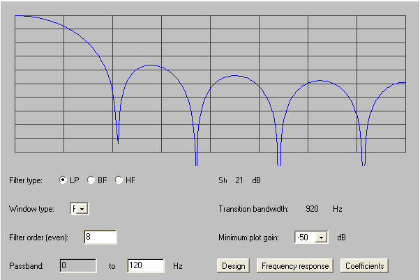
A low pass 8th order FIR has five distinct coefficients:
a[0] = 0.074217044
a[1] = 0.100043066
a[2] = 0.1210902
a[3] = 0.13484019
a[4] = 0.13961902
Fo = (s(0)+s(8))*a(0) + (s(1)+s(7))*a(1) + (s(2)+s(6))*a(2) + (s(3)+s(5))*a(3) + s(4)*a(4)
This filter involves 5 products and 8 sums, the last eight signal values must be stored and renders the frequency response below (5KHz x 50dB):
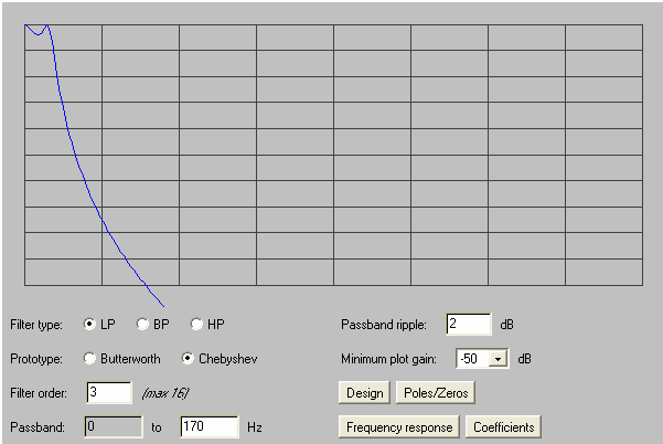
A low pass 3th order type I Chebyshev IIR has six distinct coefficients, though one of them is always 1.0. The values for a pass band from 0 to 212 Hz that allows for 2 dB of band ripple has the following coefficients.
a[0] = 9.2690025E-5 b[0] = 1.0
a[1] = 2.7807007E-4 b[1] = -2.8884988
a[2] = 2.7807007E-4 b[2] = 2.7954504
a[3] = 9.2690025E-5 b[3] = -0.90621006
The evaluated transfer function:
fo(4) = (s(4)+s(1))*a(0) + (s(2)+s(3))*a(1) - fo(3)*b(1) - fo(2)*b(2) - fo(1)*b(3)
This filter involves 5 products and 6 sums, the last 4 signal values plus the last 3 output values (totaling 7) must be stored and renders the frequency response below (5KHz x 50dB)
The formula of the IIR may involve a slightly more complex algorithm but the cutoff is a lot sharper.
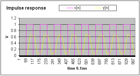
If a signal as described in the first paragraph (square wave of 85Hz), were applied to the filter, the delay would be around 30 samples, as seen above.
To be implemented in an EPLD floating point operations must be avoided. Both the input and the output signals are 10 KHz streams of 16 bit samples. Coefficients will also be will be 16 bit values, but the products and sums involved in the recurrent algorithm must be 32 bit operations.
Let the input stream be i(n) and the output stream o(n), then the recurrent formula in its integer form can be expressed as:
o(n) = (a03*(i(n-3)+i(n-0)) + a12*(i(n-2)+i(n-3)))/213
- (b1*o(n-1)+b2*o(n-2)+b3*o(n-2))/226
Where:
a03 = 8176
a12 = 24528
b1 = -23663
b2 = 22900
b3 = -7424
The algorithm involves:
The IIR above has a transition frequency of 920 Hz while the IIR cuts quite sharply around 170 Hz.
NEDT = Noise/S K°
Where S is the sensitivity in volts per Kelvin and Noise is the RMS voltage measured with a target at constant temperature.
If we consider the noise in the band from 2Hz to 1 KHz be mostly of the 1/f type, the spot noise power on the signal would be:
P(f) = K/f
The noise power after the FIR filter is then:
⌠920
PFIR = K│df/f = K(ln(920)-ln(2)) = 6.13 K
⌡2
⌠170
PIIR = K│df/f = K(ln(170)-ln(2)) = 4.44 K
⌡2
Taking the powers to RMS voltages:
VFIR = √ (R* PFIR) = 2.48 √RK
VIIR = √ (R* PIIR) = 2.11 √RK
This will render at least a 15% improvement on the NEDT. Yet, the looks of the signal on the scope will show much cleaner than the said percent.
To compensate for the digital filter delay as well as other amplifier delays (this includes that of the analog filter on the board and the RC of the video amplifier in the pixel), the relevant data capture starts with the first scan pulse and goes on an additional scan interval plus the total signal delay after the frame end pulse.
The samples that correspond to the real position at the object are not the ones immediately after the scan pulse N nor the 60 samples before the scan pulse N+1, but those being received the total delay after scan pulse N. In our case this will add up to 30 samples for the Chebyshev IIR filter plus ~2/3 of the τ of the analog filters.
The algorithm could be that of saving the entire captured sample to a buffer (~2K words). Upon receiving a scan pulse the current sample index will be saved to a 34/66 element array.
At frame start, the capture will be expender for another scan interval + Total delay. Now it would be time to build the frame, the pointer of the buffer will be incremented in 30 and the samples between scan m and scan (m+1) will be averaged and stored in the frame’s mth location.