Shows expertise in experiment design an proficiency with electronic instrumentation
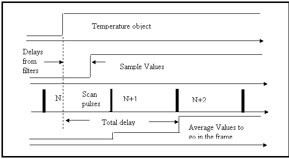
The position of a temperature object within the image frame is affected by the delays within the board. These delays are caused by:
If a temperature object is sensed between scan pulses N and N+1, the nearest average, that will start showing some effect, will be the one taken at time N+1, but will not be fully acknowledged until the average of scan pulse N+2.
The average at scan pulse N+2 goes into the N+1 row in the frame structure. This is because the DSP never gets the scan pulse 0; the first it ever gets from the EPLD is scan pulse 1 which goes into row 0. So the actual delay is less than one pixel.
We conducted the following experiment, we fed pixel 8 with a 4 Hz square wave. In the code we introduce a few lines so as to change the scope port to 1, when the average went above a threshold that we adjusted to be halfway between the minimum and maximum counts. We synchronized the scope with the square wave source on Ch1 and monitor the port with Ch 2.
The scope screen looked something like:
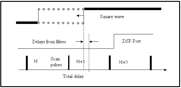
The rising edge of the square wave “moved” slowly for a scan pulse period in the indicated direction; this is because it was not exactly synchronized with the scan pulses. At the end of this “travel”, it jump to the point nearest to the DSP port rising edge.
The worst case delay will be 5.5 ms or roughly 2/3 of a scan pulse period. This is perfectly normal and can not explain the 4 vertical pixel shift reported.