Study made for the implementation of a DSP temperature control system for an array of LNA (Low Noise Amplifiers).
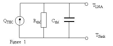
A simplified equivalent thermal circuit for the LNA (Low Noise Amplifier) system could be one as follows:
According to the TEC (TermoElectric Cooler) specs for heat sink temperature of 50°C shown below:
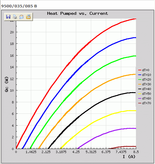
If thermally shorted (dT = 0), at 1.4 Amperes each TEC should pump 8 W, so QTEC = 8 W. If thermally opened, this is with no thermal load (Qc = 0), the temperature difference is according to the chart is:
dT = (TLNA – TSink) = 30°C.
Since there are 3 TEC’s in the parallel assembly, the thermal resistance of the TEC array is:
Rth = 30 / (8*3) = 01.25 °C/ W
The measured temperature difference at 1.4 A is actually 30°C, so the LNA to sink thermal resistance is practically that of the TEC’s.
The thermal resistance calculated for dT = 70, renders 0.93 °C/ W. This could be explained by the effect of higher carrier mobility with a lower average temperature in the semiconductor.
Considering that (1-e-1) ~2/3 of this dT vanishes in 35 seconds when PWM (Pulse Width Modulation) goes from 100% to 0%, and knowing that this decay is exponential with t/ (Rth x Cth), then the thermal capacity can also be calculated.
Cth = 35/Rth = 43.8 Joules/°C
The PID (Proportional Integral Derivative) output (pOut) PWM duty cycle delivers 1.4 Amps at 100%. At this current level, three TEC’s devices could pump P = 24 W from the LNA's according to Figure 1.
QTEC may be expressed as a function of pOut.
QTEC = P pOut [1]
On the other hand, the PID equation is:
dpOut/dt = G x (I err + derr/dt + D d2err/dt2)
or in terms of QTEC :
dQTEC /dt = GP (I err + derr/dt + D d2err/dt2) Eq 1
Where G, I and D are the PID constants: gain; Integral and derivative, respectively. The symbol err is the deviation from the target temperature in hundredth of degrees Kelvin:
err = - 100(TLNA - TTarget)
From figure 1:
QTEC = (TLNA – TSink)/Rth + Cth d(TLNA – TSink)/dt
Or its derivative:
dQTEC/dt = d(TLNA – TSink)/dt/Rth + Cth d2(TLNA – TSink)/dt2
TSink should be constant by design, this can be attained by using techniques like that of heat pipes (currently this condition is not met, so some underdamping can be expected):
d(TLNA – TSink) = d(TLNA - TTarget) = - derr/100
then,
dQTEC/dt = - 0.01(derr/dt/Rth - Cth d2err/dt2) Eq 2
Combining Equations 1 and 2:
GP (Ixerr + derr/dt + D d2err/dt2) = - 0.01(derr/dt/Rth - Cth d2err/dt2)
It takes the form of the linear differential equation of the harmonic oscillator:
kx + cdx/dt + m d2x/dt2= 0
or
I err + (1+ 0.01/ (PGRth))derr/dt + (D + 0.01Cth /(PG)) d2err/dt2= 0
Where k = I, c = (1+ 0.01/ (PGRth)) and m = (D + 0.01Cth /(PG))
The most desirable mode in a PID is that of the critical damping, that is attained when:
c = 2Ökm
or its analog;
(1+ 0.01/ (PGRth)) = 2Ö (I(D + 0.01Cth /(PG)) Eq 3
It is also desirable that all parameters of the PID have similar influence on its response. So, let’s set:
PGRth = 0.01
And
D = 0.01Cth /(PG)
Or
D =0.01 Rth Cth = 0.35 seconds
G = 0.01/ PRth = 0.00052
Then from Eq 3.
(I(D + 0.01Cth /(PG)) = 1
Or
I = 1/(2D) = 1.4 sec-1
Since the thermal capacity is bound to increase, maybe double, with the mass of the LNA's, which are currently not attached to the system, D could be expected to double and I could go half.
Introducing the electrical power dissipation within the TEC. The LNA cooler can be modeled by the thermal circuit depicted by diagram below. Though heat dissipation is distributed throughout the volume of the TEC, it we assume that this distribution is uniform, it would be equivalent to the heat being generated at a center slab.
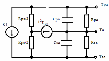
The calculation of the contribution of I2rTec to Tpa and Tsa can be simplified by considering that, by design, the thermal resistance to the ambient of the heat sink (Rsa) is much smaller than that of the LNA assembly Rpa. This means that the heat from dissipation will flow mostly through the lower part of the circuit. And so:
(Tpa)dis = (Rps/2+Rsa) I2rTec Eq 10a
(Tsa)dis = Rsa I2rTec Eq 10b
As thermal resistances of the LNA assembly to the ambient is much greater than that of the voltage driven TEC (Rps), the temperature difference Tps due to the contribution of KI is:
(Tps)KI = -Rps (KI) Eq 11
Tpa and Tsa will divide this contribution according to thermal resistances Rpa and Rsa respectively.
(Tpa) KI = Rpa/(Rpa+Rsa) (Tps)KI ~ -Rps (KI) Eq 12
(Tsa) KI = -Rsa/(Rpa+Rsa) (Tps)KI ~ (Rsa/Rpa) Rps (KI) Eq 13
Adding contributions for Tpa:
Tpa = (Tpa)dis + (Tpa)KI
Or
Tpa = (Rps/2+Rsa) rTec (I2 - (Rps/((Rps/2+Rsa) *rTec)K I) Eq 14
The equation above may be put into the form:
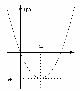
Tpa = Tmin/Itm2((I – Itm) 2 - Itm2) Eq 15
Where :
Itm = (Rps/2/(Rps/2+Rsa)) (K/rTec) Eq 16
and
Tmin = (Rps/2+Rsa) rTec* Itm2 Eq 17
Let’s throw in some numbers:
From figure 1, three TEC’s can deliver a net pumping of 24 W with 1.4 Amps. The total heat pumping would be the net capacity plus the electrical dissipation that take part of the whole pumping capacity:
K = (24W+I2* rTec )/1.4A W/A
On the other hand, Total thermal resistance from p to s, that is Rps || (Rpa+Rsa) was measured to be 1.25 °C/ W at higher temperatures. Since Rpa is expected to be greater than all the rest, Rps is very much 1.25 °C/ W.
At any moment in time, the voltage on the TEC’s is the sum of the thermal EMF plus voltage drop on the internal electrical resistance rTec. If, at some point in time, the circuit is opened, only the thermal EMF with remain, the drop in voltage being that on rTec.
Vdrop = I rTec
This value went from 3.85W to 6.34 W as the current went from.013A to 1.3A and sink temperature went from ambient 25°C to + 45°C. This experiment doesn’t allow establishing if the observed change in internal resistance is due to it being a function of I or of Tsa.. Yet, from semiconductor physics we know that in PN junctions currents behave exponentially with the applied voltage; this would render a monotonic decrease in resistance contrary to what is observed. On the other hand, charge carrier mobility decreases with temperature; this could acount to for the observed ohmic increase,
Assuming that figure 1 was obtained under the best case scenario conditions of a perfect heat sink (Rsa = 0). If we used the smallest measured value for rTec and Rps.
K = 22.5 °C/ W
Imin = 5.8 A
Tmin = 60 °C
But for the greatest rTec and Rps, then the set of values is quite different.
K = 26.0 °C/ W
Imin = 3.3 A
Tmin = 42 °C
Being this the most likely set of values, the Tpa at 1.4 A will be only 28°C, so the system may not be able to control the requested 30°C with an ambient temperature of 60°C. Increasing the number of TEC’s is not a solution, since the only thermal load being considered in this analysis is that of the TEC’s themselves, increasing the pumping capacity with more TEC’s will equally increase the thermal load. Adding a thermal load to the system, even the 1.2 W from the 32 LNA quiescent points, could further worsen the system operating temperature range.
The actual experimental values for our current system where:
Imin = 1.3 A
Tmin = 15 °C
Going backwards to check consistency, using Eq 16 and the value for rTec, measured a 1.3 A, the thermal resistance of the heat sink to the ambient must be:
Rsa = 1.5 °C/ W
Using this value in Eq 17 you get 20.36 °C for Tmin which is not far from the experimental value. Now, combining equations 10b and 13 we get an expression for Tsa:
Tsa = Rsa(I2rTec + KIRps/Rpa)
Or, solving for Rpa:
Rpa = KIRps /(Tsa/Rsa - I2rTec)
Since the observed Tsa was 45°C, evaluating, we get a value for Rpa that is consistent with the assumption Rpa >> Rsa to roughly 10% accuracy:
Rpa = 11.3 °C/ W
Implement a measurement of what would be the highest operating temperature for the system. If results were to be considered insufficient, then a circuit with more power must be designed.
[1] pOut is actually a voltage PWM duty cycle. Voltage is not linear with the current and the current is not linear with the heat pumping either. Non linearity will render different damping conditions with different temperature swings. A better approximation could be derived further on